Difference between revisions of "Change: Interface PCB"
(→Background) |
|||
| Line 2: | Line 2: | ||
==Background== | ==Background== | ||
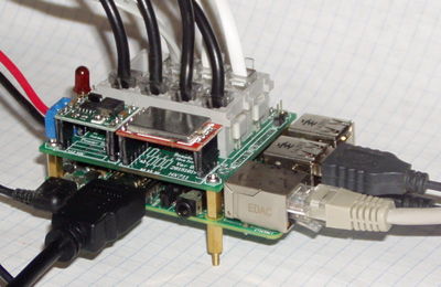
A Printed Circuit Board (PCB) has been designed and manufactured. | A Printed Circuit Board (PCB) has been designed and manufactured. | ||
| − | The goals were to make it quicker and easier to build a system and to make it more reliable, to establish a relationship with a board house and to test the | + | The goals were to |
| + | #make it quicker and easier to build a system and to make it more reliable, | ||
| + | #to establish a relationship with a board house and | ||
| + | #to test the footprint of the RJ connectors and mating with the Pi | ||
| + | #to select a pcb layout package. | ||
| + | This is an interim solution - a step towards the goal of a complete turnkey system. | ||
*All sensor plug in. | *All sensor plug in. | ||
Revision as of 19:09, 7 December 2015
Background
A Printed Circuit Board (PCB) has been designed and manufactured. The goals were to
- make it quicker and easier to build a system and to make it more reliable,
- to establish a relationship with a board house and
- to test the footprint of the RJ connectors and mating with the Pi
- to select a pcb layout package.
This is an interim solution - a step towards the goal of a complete turnkey system.
- All sensor plug in.
- 12 VDC power supply with battery voltage monitoring
Problems
- ADC is only one channel.
- No RTC
- Board does not meet Pi HAT spec
Proposed change
Split this board in two.
- One board will meet the Pi HAT specifications and contain:
- at least one 4 channel ADC so each load cell will be individually measured instead of being summed.
- Real Time Clock with battery backup.
- Configuration ROM
- One board will have all the connectors installed in a bulkhead configuration.
